logo
좋은 가격  온라인

제품 세부 정보

Created with Pixso. Created with Pixso. 제품 Created with Pixso.
IC 실리콘 박편
Created with Pixso. SOI Wafer:Lower parasitic capacitance stronger latch-up immunity improved radiation resistance

SOI Wafer:Lower parasitic capacitance stronger latch-up immunity improved radiation resistance

브랜드 이름: ZMSH
모델 번호: 소이웨이퍼
MOQ: 25
가격: Fluctuates with market
배달 시간: 2~4주
지불 조건: 티/티
자세한 정보
원래 장소:
중국 상하이
재료:
이산화규소(SiO2)/실리콘(Si)
웨이퍼 지름:
맞춤형
장치 레이어 두께:
맞춤형
BOX 층 두께:
맞춤형
결정 방향:
<100> / <110> / <111> / 맞춤형
도전성 타입:
N형 / P형 / 맞춤형
제품 설명
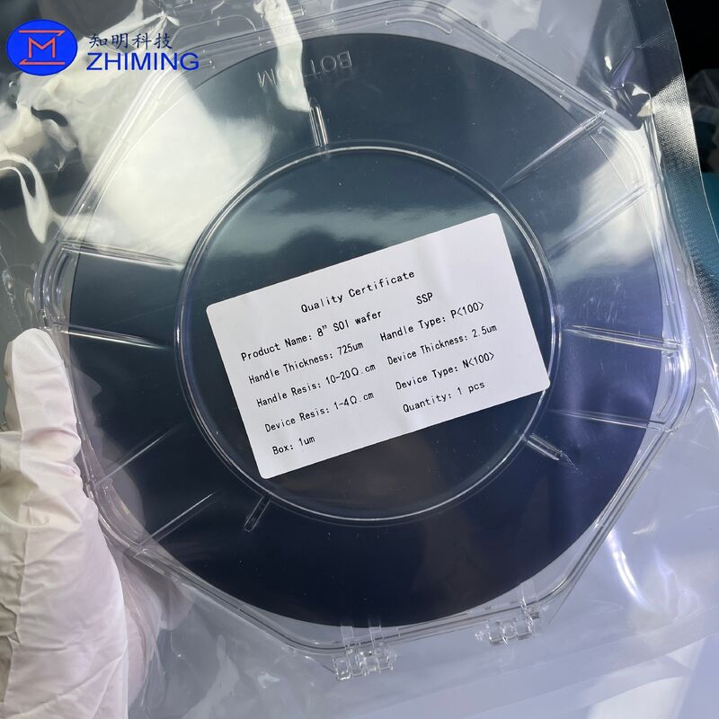
Product Information SOI (Silicon-on-Insulator) is a “sandwich” structure wafer consisting of three layers: the top silicon layer, also known as the Top Si / Device Layer, is used to fabricate transistors; the middle layer is the Buried Oxide (BOX), which provides electrical isolation; and the bottom layer is the silicon support substrate (Handle/Substrate Wafer). Compared with conventional Bulk Si wafers, SOI wafers feature complete dielectric isolation, enabling lower